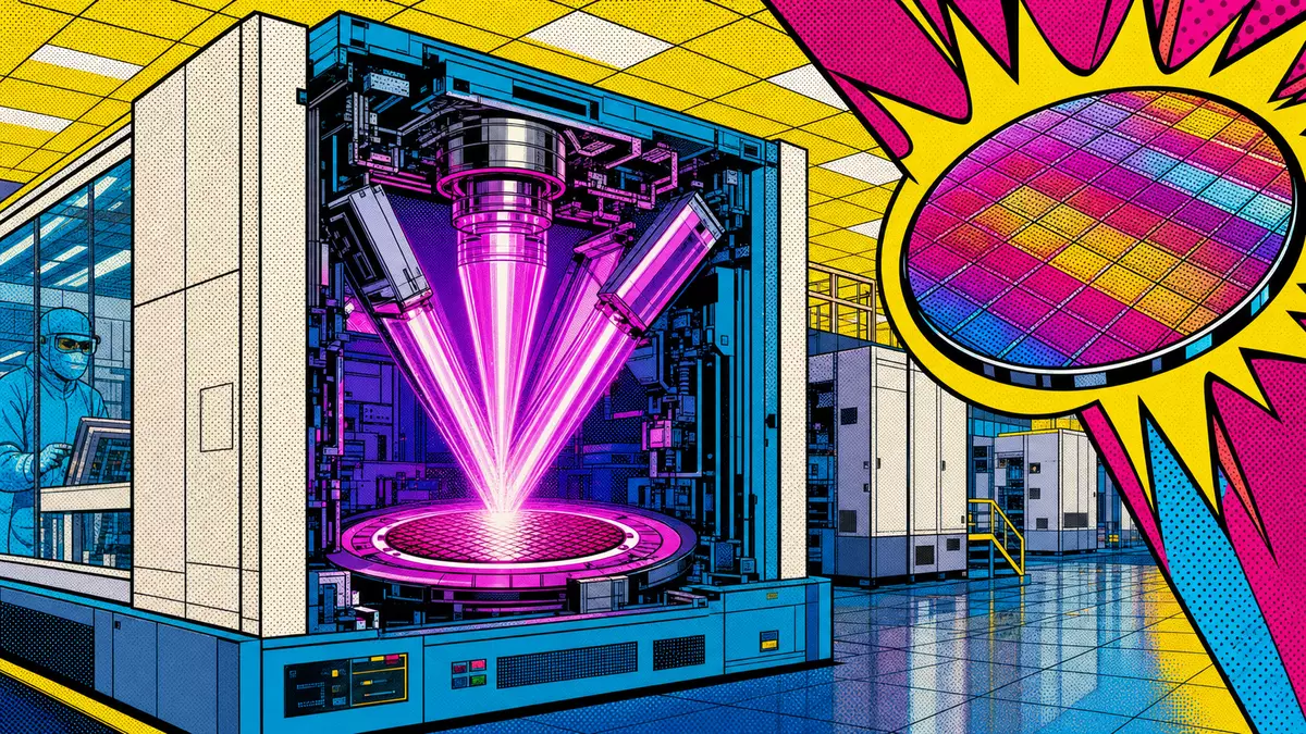
The PAS 5500 lithography system. ASML holds on to a proven workhorse
Published on 07/26/2026 at 12:05 | Editorial responsibility: Rafael Müller, Editor-in-Chief AD HOC NEWS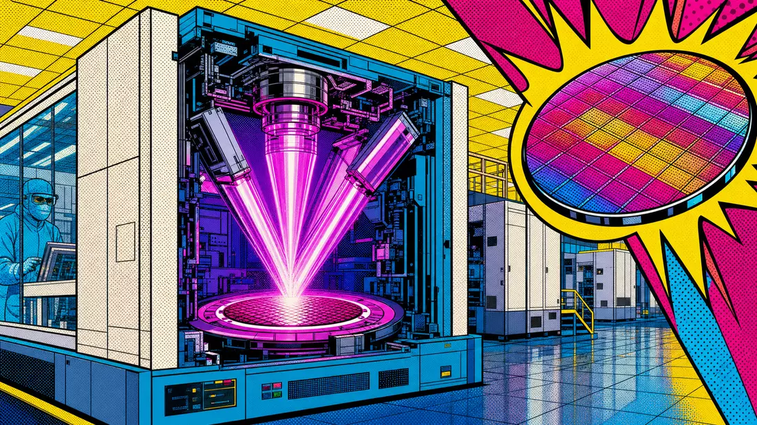
The PAS 5500 lithography system stands in the middle of the cleanroom, its beige side panels slightly worn, cables tucked underneath, and a low mechanical hum mixing with the rush of filtered air. An engineer in a blue bunny suit leans in, watching the wafer handler glide a 200 mm wafer under the projection lens with surgical precision.
Mature-node workhorse in ASML’s line-up
ASML launched the PAS 5500 family in the 1990s as a key 200 mm wafer lithography platform for logic and memory chips on mature technology nodes. These systems cover a wide range of i-line, g-line and deep UV step-and-scan configurations for processes roughly from 0.7 µm down to about 0.18 µm, depending on the exact variant. Even today, PAS 5500 scanners remain in use for automotive, industrial and power semiconductor production, where proven stability and predictable yields matter more than pushing the absolute resolution frontier.
On ASML’s overview of installed base and service offerings, PAS 5500 appears as part of its "mature products" segment, alongside other non-EUV lithography systems. That segment is a meaningful business: ASML notes in several investor presentations that service and field upgrades on systems like PAS 5500 contribute a recurring revenue stream, especially as fabs stretch the lifetime of 200 mm lines for analog and mixed-signal chips. This is not the flagship Twinscan or the highly visible NXE EUV series – instead, PAS 5500 is the workhorse quietly keeping capacity online in older fabs.
How a PAS 5500 scanner works day to day
ASML’s PAS 5500 systems are projection lithography scanners that use a high-precision stage to move the wafer under a projection lens while stepping and scanning the reticle image. Typical deep UV variants use KrF excimer laser sources at 248 nm wavelength, paired with advanced projection optics to deliver sub-0.25 µm resolution on 200 mm wafers. Earlier g-line and i-line PAS 5500 tools rely on mercury lamps and different lens configurations, targeting larger feature sizes but offering robust process windows for specialty devices.
Inside the tool, a robotic wafer handler moves each wafer from its cassette into the exposure chamber, while sensors constantly monitor focus and alignment. The stage under the lens accelerates and decelerates with micrometer precision, and the reticle – a glass plate with the chip pattern – is scanned in sync to print each die across the wafer surface. Engineers like process integration manager Jan van der Meer at a typical European analog fab spend their day tweaking exposure dose, focus offsets and overlay parameters so that the PAS 5500 keeps hitting tight line-width and alignment specs on every batch.
ASML’s mature lithography business in focus
How the PAS 5500 installed base, field upgrades and service tie into ASML’s recurring revenue and long-term margin profile.
Installed base, lifecycle and service
ASML highlights its installed base management program as a core pillar of its strategy, covering systems like PAS 5500 with field service, performance upgrades and refurbishment options. In its annual reports, the company notes that installed base revenue, which includes service contracts and upgrades, has grown significantly over the last decade as chipmakers extend the operational life of existing tools. PAS 5500 scanners benefit directly from this trend: rather than being scrapped, many are upgraded with improved software, new illumination options or tighter overlay control modules.
According to ASML’s published product lifecycle documentation, mature tools such as the PAS 5500 pass through phases of active sale, limited sale and eventually service-only support. While new PAS 5500 systems are no longer a standard catalogue item, the company maintains service coverage and spare parts availability for a large population of installed systems worldwide. That includes customers in Europe, Asia and the Americas who rely on 200 mm lines to manufacture automotive MCUs, power transistors, sensors and RF components. For a production manager like Li Wei at a Chinese analog fab, keeping a PAS 5500 running with minimal downtime often matters more than chasing the latest EUV capability.
Use cases: from cars to power grids
Most PAS 5500 systems today are used at technology nodes between roughly 0.35 µm and 0.18 µm in specialty processes. These include high-voltage power ICs, motor drivers, microcontrollers for airbags and engine control units, and mixed-signal chips for industrial automation. In these segments, design rules are stable and certified for safety standards, so fabs are reluctant to move production to newer nodes that would require lengthy requalification.
Industry reports from market research firms such as IC Insights and TechInsights describe a shortage of 200 mm capacity during recent semiconductor cycles, driven by strong demand for analog and power devices. Tools like PAS 5500 are part of the backbone of that capacity. While the headlines focus on EUV and 3 nm logic, a PAS 5500 quietly patterns the gate structures for a 0.18 µm automotive MCU that will sit in a car’s braking system for a decade. The tactile reality is that each wafer leaving the tool feels like a smooth, slightly warm disc, its future chips invisible but already defined in photoresist.
Technology context inside ASML’s portfolio
Within ASML’s broader portfolio, PAS 5500 occupies the mature-node niche below the more recent Twinscan scanners for 300 mm wafers and above older PAS 2500 series tools. In the company’s product family lists, PAS 5500 is grouped under "KrF, i-line and g-line" systems, distinguished from ArF immersion tools and EUV platforms. ASML’s CEO Peter Wennink has repeatedly pointed out in earnings calls that the company’s earnings do not only come from leading-edge EUV, but also from supporting customers across all nodes, including mature logic and analog.
Analysts at firms like Bernstein and UBS have noted in their coverage that mature-node demand, including 200 mm lines, helped stabilize ASML’s order intake during periods when leading-edge investments slowed. Orders for new EUV or high-NA EUV units may fluctuate with the logic foundry cycle, but service and upgrade revenue on installed tools like PAS 5500 tends to be more resilient. In that sense, the continued presence of PAS 5500 systems across many fabs forms part of the company’s earnings ballast.
How PAS 5500 compares with newer scanners
Technically, PAS 5500 scanners cannot match the throughput or resolution of modern Twinscan or EUV systems designed for 300 mm wafers and sub-10 nm nodes. A typical PAS 5500 deep UV system specifies throughput around 100–120 wafers per hour for 200 mm wafers, depending on exposure settings and process complexity. In contrast, modern Twinscan NXT platforms, as described on ASML’s product pages, target significantly higher wafer-per-hour numbers on larger wafers.
However, the older tool’s economics look different: PAS 5500 has lower acquisition cost on the secondary market, and its process recipes are stable and well understood. For a fab running mostly 0.35 µm analog or power devices, this can be the optimal balance. Comparisons from refurbishers such as Canon Anelva and used equipment brokers show that demand for 200 mm scanners remains elevated, with PAS 5500 models among the desirable units for capacity expansions in mature-node fabs.
Revenue impact and stock context
ASML breaks down its revenue between new systems and installed base management in its annual reports and investor presentations. While it does not publicly split revenue by individual product line such as PAS 5500, the installed base category includes service fees, spare parts and upgrades across all legacy platforms. Given the still sizeable fleet of PAS 5500 scanners, especially in Asia and Europe, their maintenance and optimization contributes to this recurring revenue pool.
ASML Holding N.V. share is listed on Euronext Amsterdam, trading in euro under ISIN NL0010273215. For investors, the PAS 5500 systems are part of the behind-the-scenes machinery supporting ASML Holding N.V. stock as a combination of leading-edge EUV growth and mature-node stability.
Key facts: PAS 5500 lithography system
- Product: PAS 5500 lithography system
- Manufacturer: ASML Holding N.V.
- Category: Classic / Longseller lithography system
- Market launch: First PAS 5500 systems introduced in the 1990s for 200 mm wafer fabs.
- MSRP / Price: No current official list price; traded mainly as refurbished equipment in the secondary market.
- Availability: Installed base in fabs worldwide; supported by ASML through service and upgrades, occasionally available as refurbished systems.
- Target group: Semiconductor manufacturers running 200 mm lines for mature-node logic, analog, power and automotive chips.
- Highlight / USP: Proven, stable 200 mm lithography platform for mature nodes, backed by ASML’s installed base service and upgrade programs.
Disclaimer regarding our articles: No investment advice, no buy or sell recommendation. Information on prices, companies, and markets is provided without guarantee; changes are possible at any time. Stock market transactions can lead to substantial losses. Our articles are created and reviewed in whole or in part automatically with the support of AI.